Potomac Photonics is proud to help our neighbors at bwtech@UMBC

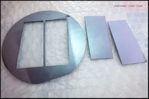
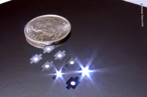
Wafer dicing has been used for decades in the semiconductor industry to separate the individual die, or integrated circuits, from the large wafers on which they are manufactured. Often the wafer is scribed and then mechanically broken apart or sawed with special tools. However, laser cutting is the process of choice when high precision separation without damage to the substrate is required.
Potomac’s neighbor at the Research & Technology Park bwtech@UMBC, Blue Wave Semiconductor, recently came to us needing high precision wafer dicing. Blue Wave builds semiconductor tools that use wafers as the foundation for their thin film technology. Explains company founder Dr. R. D. Vispute, “Blue Wave can build advanced devices on one wafer and silicon is a desirable platform for creating fast prototypes. Silicon is a very common material, making it easy to commercialize.”
Blue Wave’s technology requires customized chip sizes on the silicon wafers for which specific geometric form factors are required to optimize performance. Dr. Vispute says “cutting silicon in appropriate forms and shapes is tricky because 500 micron thick silicon is fragile. Plus being a single crystal material, there is a preferred direction to the structure, creating the possibility of cracking. Because laser cutting does not damage the substrate, I felt it was the best way to go for our wafer dicing application.”

Potomac utilizes a wide range of lasers operating at a variety to wavelengths from the infrared to the ultraviolet, allowing us to choose the right laser for the job. Depending upon the feature size, thickness of the material, absorption, and other factors, we can optimize the process for the specific application’s parameters. “Over the years, we’ve developed some of the most advanced and cost-effective processes, fixturing and other techniques related to micro manufacturing ,” says Potomac President and CEO Mike Adelstein, “that create the best quality result for our customers’ demanding applications.”
Dr. Vispute for one was impressed by the quality of the work, saying, “There was minimal damage to the silicon and the efficiency was very high. The rapid turnaround allowed me to quickly test our prototypes which greatly impacts time to market.” And for Potomac, helping our customers get innovative products to market quickly ensures everyone’s success.


