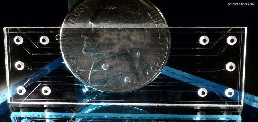
Potomac Photonics is pleased to have partnered with the Budker Group at the Physics Department of the University of California, Berkeley on a recent project. The Budker Group conducts research on the physics and applications of ensembles of nitrogen-vacancy (NV) centers in diamond to detect magnetic fields with high spatial resolution. One possible application is to mount diamond sensors on board microfluidic chips in order to detect magnetic particles traveling in the microfluidic channels. This requires precision custom drilling of thin glass windows through microfluidic chips. Drilling on this scale with the required accuracy is difficult to accomplish with traditional techniques. Potomac Photonics was able to utilize advanced manufacturing techniques to drill small holes in the glass coverslips of these microfluidic devices to provide the researchers with access to the channels for their experiments.
For over 30 years, Potomac Photonics has been a leader in microfabrication and small hole drilling. Potomac’s contract services span prototyping to production, helping clients develop miniature products and bring them to market. Using cutting-edge manufacturing technology, Potomac has been recognized by both commercial and government agencies for innovation in areas such as medical device, electronics, aerospace, and automotive manufacturing. Potomac’s high-tech facility, located in Lanham, MD, is ISO 9001:2008 and ISO 13485:2003 certified. Visit the website at www.potomac-laser.com


