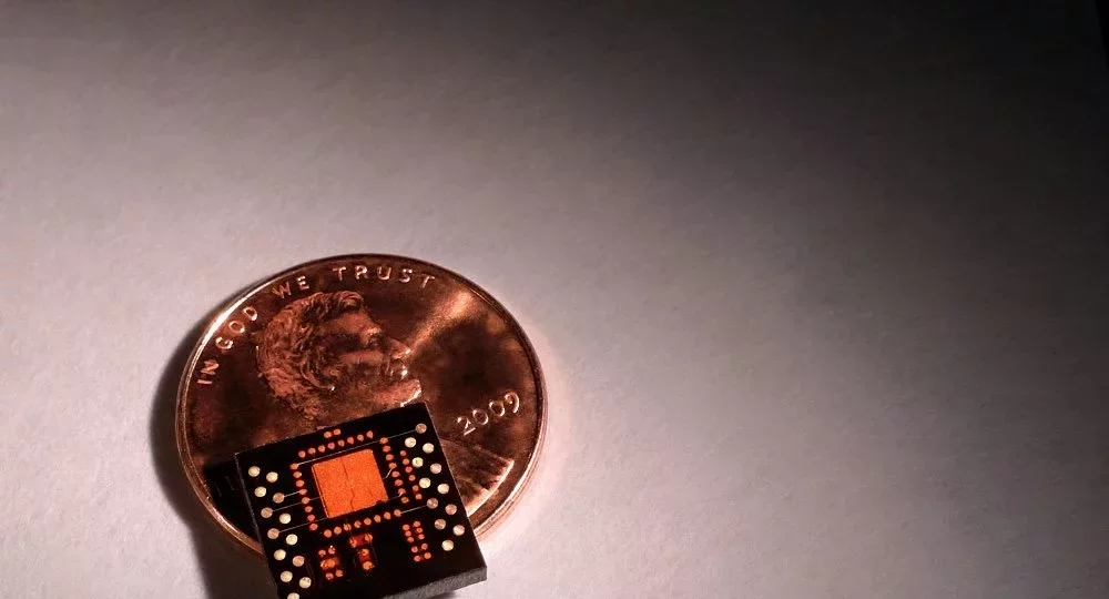
The article describes new techniques that combine laser fabrication with conductive nanoparticle materials, allowing further miniaturization of electronic devices among other benefits.
Lanham, MD, May 22, 2013 – Micro-hole drilling expert Potomac Photonics was recently featured in PCB Magazine’s May issue that was centered on small hole formation and processing. Potomac’s article Looking Outside the Hole: the Evolution of Via Drilling explained a new laser fabrication process developed to spur miniaturization of electronic devices.
Potomac Photonics is a pioneer in the use of ultraviolet lasers for laser fabrication, especially micro-hole drilling, via drilling, micromachining and marking. Over a period of three decades Potomac has developed expertise for via drilling in a variety of substrates including organic polymers such as Kapton, metals, ceramics, silicon and glass. Manufacturing knowledge allows for either blind or through micro-hole drilling without damage to the substrate, and with high precision in hole diameter and pitch.
The work described in the PCB Magazine article describes new miniaturization techniques that combine laser fabrication of channel patterns and via drilling with conductive nanoparticle materials to form traces in the 10-micron range. The innovative laser fabrication process solves the problem of hole size limitations in traditional PCB manufacturing, for further miniaturization of electronic devices. Mike Adelstein, President and CEO of Potomac, is “excited by the possibilities of the Mill and Fill process. Applications in micro-wireless sensors, mobile platforms and consumer products can now be addressed that we could not have imagined just a few years ago.”
Size reduction of electronic devices is an important result of the unique process, but there are additional benefits as well. Dr. Paul Christensen, whose company, Potomac MesoSystems developed the process jointly with Potomac Photonics, explains that “forms we can produce are no longer limited to 2D. We can make a variety of shapes and geometries, and even create electronic devices on conformal surfaces. Potomac’s laser fabrication technique also allows for easier miniaturization of flex circuits, essentially making it a ‘smart’ interconnection device.”
Because of its additive manufacturing properties, Mill and Fill via drilling reduces the need for consumables and it is a more “green” process. The circuit board assembly utilizes proprietary processes at lower temperatures and without the use of lead. Micro-hole drilling in the ultraviolet is essentially an ablative process with less debris generated than in thermal processes. Recent advances in solid state lasers have increased through-put, making laser micro-hole drilling competitive from a cost perspective.
Potomac Photonics’ combination of laser micro-hole drilling with nanotechnology is clearly poised to drive miniaturization of electronic devices across industries. To read the entire article, Looking Outside the Hole: the Evolution of Via Drilling, on the Potomac website.
About Potomac Photonics
For over 30 years, Potomac Photonics has been a leader in microfabrication and small hole drilling. Potomac’s contract services span prototyping to production, helping clients develop miniature products and bring them to market. Using cutting-edge manufacturing technology, Potomac has been recognized by both commercial and government agencies for innovation in areas such as medical device, electronics, aerospace, and automotive manufacturing. Potomac’s high-tech facility, located in Lanham, MD, is ISO 9001:2008 and ISO 13485:2003 certified. Visit the website at http://www.potomac-laser.com


