In the last few years, microfluidics has come into its own as a process and also a micro-manufacturing technology. The methodology is rapidly changing many diverse fields from Point-of-Care diagnostics to cancer research, environmental studies to Organs-on-a-Chip, drug discovery to micro fuel cells, and much more. By using a small drop of fluid, microfluidics speeds up detection times, increases sensitivity and for medical applications, opens new opportunities for medicine to be more humane.
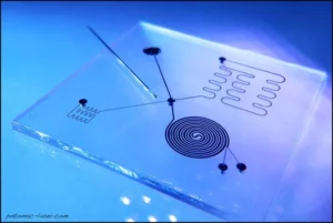
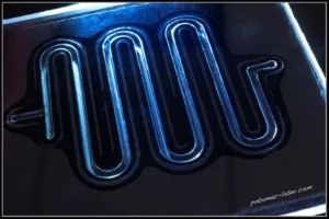
In microfluidic devices, tiny amounts of fluids are processed in a system of small channels that can be as small as 10 microns in width and depth. While there is a lot of interest in the manufacture of these channels, other features of microfluidic device fabrication require manufacturing innovation as the field progresses into new applications.
Drilling Holes In Microfluidic Coverslips

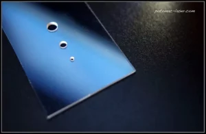
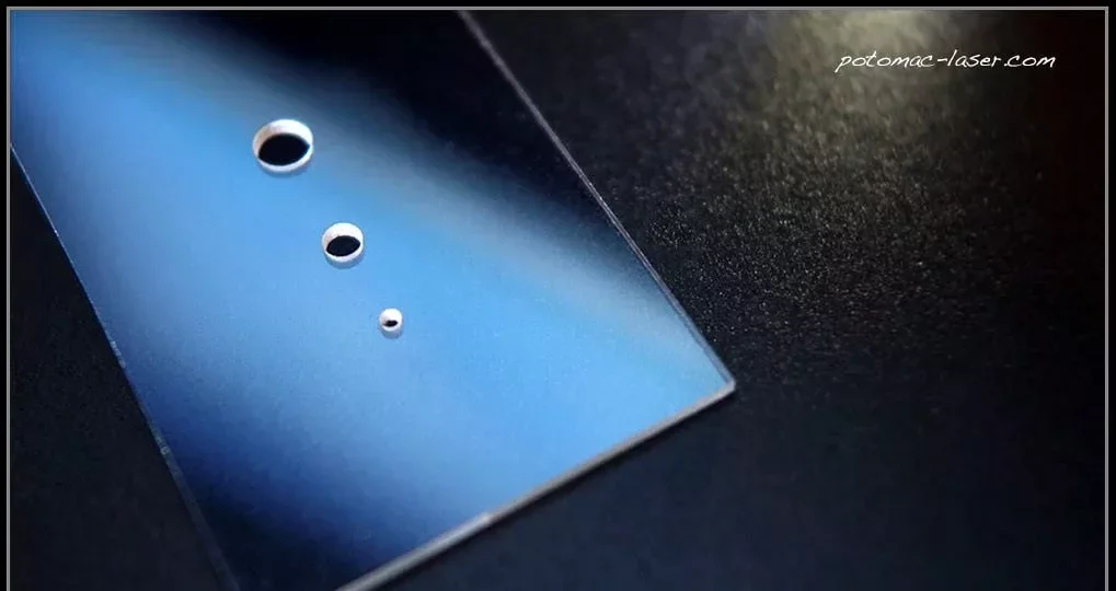
Microfluidic device channels need to interface with the outside world for a variety of tasks. Fluids and sometimes gases need to be added or removed from the channels, and connections need to be made to external components of the system. Hole size typically ranges from 200 um to 2 mm and placement must be accurate. Most significantly, Potomac can now drill holes in 1mm thick materials.
For both glass and organic polymer coverslips, Potomac has developed novel processes to manufacture devices. There are many types of glass, but all are hard and brittle solids. While these are good qualities for many applications, it is what makes glass difficult to machine. Working closely with our customers, we have developed specialized techniques to machine glass without damage or cracking. This is especially important for the very thin glass coverslips that are used in biotech and medical microfluidics device applications.
Polymers absorb strongly in the UV region of the laser light spectrum and are machined by a process known as photoablation. Rather than thermally cutting through the material, the covalent bonds are broken by the UV laser interaction with the material. Polymers literally fly apart and the benefit is the lack of thermal damage to the substrate. Consequently, UV laser micromachining of polymers yields beautiful edge quality. With more use of COC and PMMA in microfluidic device fabrication, UV laser machining is an important tool in the manufacturing process.
Bonding for Microfluidics

Sealing microfluidic device components is usually achieved by bonding. Potomac has worked with the biotech and medical research communities to develop innovative bonding techniques, especially for polymers and thermoplastics. The simplest and most cost-effective available technique is via pressure sensitive adhesive (PSA) layers. Adhesive bonding is another option where layers of medical grade adhesive materials are first precisely patterned with a UV laser to allow inter-connection between the device layers. The adhesive sheets are then aligned and laminated between the device layers. In order to improve the bonding quality and strength, a final specialty post-processing step is added which literally “seals the deal”. Alternative bonding technologies, include solvent-assisted bonding, thermal bonding, and laser welding, are all available from Potomac.
With consultation on your specific application, we can provide advice on the process that is best for you and expedite your microfluidic device fabrication.


