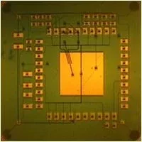
Potomac’s broad-range of micro manufacturing technology includes a novel technique to embed conductive materials in a wide variety of substrates.
Using laser-based processes, Potomac can produce fine-feature groove and channel patterns in many electronics and display substrate materials. We can then fill these etched patterns with a nanoparticle silver paste which is cured at low temperatures to produce fine-feature conductor patterns embedded into the substrate.
The cured nanoparticle materials exhibit high electrical conductivity, and minimum feature sizes can be 10 microns or less. Aspect ratios (height/width) can be larger than 1. Conductors with these characteristics are difficult to fabricate with conventional jet-printing or etching processes.
Conductor patterns can be fabricated on both top and bottom of the substrate with silver-filled vias providing connections between them. The combination of fine feature sizes and a via interconnect capability gives embedded nanosilver conductor technology a significant advantage in many applications


