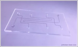
Stanford researchers find the flexibility and affordability of the Fast Track program the right fit for R&D in biotech microfluidics project.

July 9, 2015; Baltimore, MD: Fast Track, recently introduced by Potomac Photonics specifically for affordable microfluidics device fabrication, has expedited research to advance biotech applications in the Materials Science and Engineering Department at Stanford University. Fast Track gives quick turnaround and economical microfluidic device solutions, which is key to optimizing designs in the R&D phase.
Researchers at Stanford Microfluidics Laboratory led by Juan Santiago have developed a novel approach to creating new nanostructures used to study physiology and disease pathology at the cellular level. While current detection methods yield high accuracy, these mature technologies often kill the cells, requiring additional time-consuming steps to get accurate results. Modifying the physical structure of an electroporation system with 200 x 200 micron nanostraw microwells allows Stanford researchers to locally sample very small, highly concentrated groups of cells.
PhD Candidate Yuhong Cao contacted Potomac as the entire nanostraw microwell structure needed to sit atop a 100 micron wide by 5 cm long microfluidic channel. Ms. Cao explains: “To form a noninvasive electroporation, 20V pulses are applied at 20Hz between the cell culture reservoir and TE reservoir for one minute. Only the cells in contact with the microwell experience the electric field to be porated. The released GFP molecules diffuse across the nanostraw membrane to the TE channel, and are pre-concentrated by ITP. The green fluorescence intensity in the ITP zone is collected by a CCD camera to measure the results.”
The Fast Track program was perfect for Ms. Cao’s experiment because it is CAD-based and software driven, allowing for quick and easy design adjustments, an idea endorsed by Ms. Cao when she stated, “The main benefit is the flexibility. I can custom design a channel and see the change in my results at a very reasonable price. Other techniques are prohibitively expensive, given my R&D budget.”
According to Potomac CEO Mike Adelstein “Potomac developed the Microfludics Fast Track program with the primary goal of removing barriers for researchers, start-ups and biotech companies to develop and bringing new devices to market quickly. We are committed to providing our partners the fastest and most cost-effective tools to fabricate custom microfluidic chips”.
For this particular experiment, organic polymers such as PMMA yield good results and the parameters fit easily into the Fast Track program’s guidelines of a minimum 50-micron wide and maximum 200-micron deep channel dimension. Staying within Fast Track’s design requirements keeps pricing low, however custom designs outside the program are easily manufactured in Potomac’s standard microfluidic device fabrication system.
About Potomac Photonics
For over 30 years, Potomac Photonics has been a leader in microfabrication, laser micromachining and small hole drilling. Potomac’s contract services span prototyping to production, helping clients develop miniature products and bring them to market. Using cutting-edge manufacturing technology, Potomac has been recognized by both commercial and government agencies for innovation in areas such as medical device, electronics, aerospace, and automotive manufacturing. Potomac’s high-tech facility, located at BWTech@UMBC Research and Technology Park, is ISO 9001 and ISO 13485 certified. Visit the website at www.potomac-laser.com


